
Future devices will continue to probe the frontier of the very small, and at scales where functionality depends on mere atoms, even the tiniest flaw matters.

Researchers at Rice University have shown that hard-to-spot defects in a widely used two-dimensional insulator can trap electrical charges and locally weaken the material, making it more likely to fail at lower voltages. The findings are published in Nano Letters.
“By showing practical ways to detect when and where these defects form, we help make future devices more reliable and repeatable,” said Hae Yeon Lee, an assistant professor of materials science and nanoengineering at Rice who is a corresponding author on the study.
Building ultrathin electronics such as advanced transistors, photodetectors and quantum devices involves stacking sheets of different 2D materials on top of each other into “heterostructures.” Hexagonal boron nitride (hBN), prized for being atomically flat and chemically stable, is a common building block.
“A material’s strength, color and electrical behaviors come from the way its atoms are arranged,” Lee said. “However, real materials are not perfect. In hBN, we found that long, narrow misalignments can occur ⎯ similar to the creases that form when a few pages in a book have slipped. These hidden defects form easily and are just as easy to miss.”
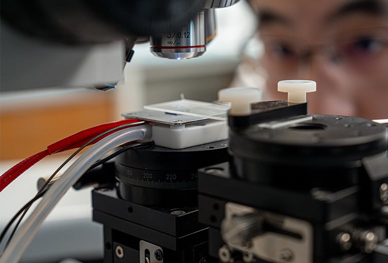
The researchers peeled thin hBN flakes from a bulk crystal using adhesive tape, then transferred them onto silicon and silicon dioxide wafers. They suspected that this routine handling might bend the sheets, causing defects called stacking faults.
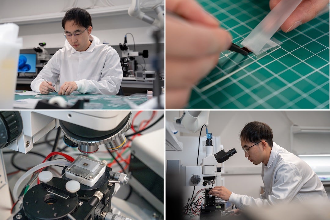
“To test this, we imaged the same hBN flakes before and after transfer,” Lee said.
Under a regular optical or atomic force microscope, the flakes looked smooth and pristine. Next, at Rice’s Shared Equipment Authority, they examined the samples using cathodoluminescence spectroscopy ⎯ a technique that scans a material with an electron beam and records the light it emits.
“hBN emits deep ultraviolet light that many labs cannot easily excite,” Lee said. “This emission map revealed bright, narrow stacking faults that other methods miss ⎯ one reason they have been overlooked.”
The faults form more readily in thicker flakes. Moreover, the change in structure causes a change in material performance.

“These hidden defects act like tiny charge pockets and weaken insulation: The same hBN can start leaking electricity at much lower voltage along the defects than nearby areas,” Lee said.
That means that two devices built the same way can behave differently if one contains these fault lines.
By combining electron microscopy, cathodoluminescence mapping and force-based measurements, the team developed a practical way to spot these defects before they undermine a device. The approach can also be applied to other layered materials.
The research was supported by the U.S. Army Research Office (W911NF-25-1-0265), the Japan Society for the Promotion of Science (KAKENHI 21H05233 and 23H02052), the Japan Science and Technology Agency (JPMJCR24A5), Japan’s World Premier International Research Center Initiative and Japan’s MEXT Scholarship. The content in this press release is solely the responsibility of the authors and does not necessarily represent the official views of funding entities.
- Peer-reviewed paper:
-
Hidden stacking fault charge traps in hBN and their impact on dielectric breakdown | Nano Letters | DOI: 10.1021/acs.nanolett.5c06347
Authors: Tian Lang, Yifeng Liu, Aryan Chugh, Kenji Watanabe, Takashi Taniguchi and Hae Yeon Lee
https://doi.org/10.1021/acs.nanolett.5c06347 - Access associated media files:
-
https://rice.app.box.com/s/tqh9gs2rhohcrqbtzs2kwnylqk8ih4gu
Credit: Photos by Jorge Vidal/Rice University