NEWS RELEASE
Editor’s note: Links to video and high-resolution images for download appear at the end of this release.
David Ruth
713-348-6327
david@rice.edu
Mike Williams
713-348-6728
mikewilliams@rice.edu
Microscopic ‘donuts’ a treat for quantum tech
Rice U., Oak Ridge scientists study potential of synthetic strain engineering in 2D materials
HOUSTON – (June 3, 2019) – Dedicating dollars to “donuts,” scientists at Rice University are helping a national laboratory bring about a revolution in electronics and, perhaps, quantum computing.
By patterning nanoscale donuts into a two-dimensional crystal, researchers at Oak Ridge National Laboratory and their colleagues, including theoretical scientists at Rice’s Brown School of Engineering, have achieved a new level of control over its electrical and optical properties.
A model by Rice University shows how compressive strain (blue) and tensile strain (red) form as a growing two-dimensional crystal conforms to a micron-scale “donut” pattern on a substrate. The strain makes the hole a semiconductor and a possible source of single-photon emission. Video by Nitant Gupta/Henry Yu/Yakobson Research Group
As researchers eye nanoscale materials for applications like quantum information processing, a method to tailor them from the bottom up will make them more practical.
The research team, which includes Rice materials theorist Boris Yakobson and graduate students Nitant Gupta and Henry Yu, published its results in Science Advances.
Oak Ridge scientists led by David Geohegan, Kai Xiao and Kai Wang first grew 2D tungsten disulfide via chemical vapor deposition on a flat substrate patterned with sharp steps and trenches and curved in only one direction. The crystal easily conformed to the obstacles without any change to its properties.

Growing two-dimensional crystals over an array of micron-scale “donuts” may lead to tailored materials for quantum information processing and other novel electronics, according to scientists at Oak Ridge National Laboratory and Rice University. Illustration by Henry Yu
But when they made the supporting surface a dome or a well — in scientific terms, a “non-zero” Gaussian curvature — the growing crystal was forced to adjust by stretching or contracting. An outward curve added tensile strain and shrank its electrical bandgap to change its semiconducting properties. An inward curve added compressive strain, making it a stronger insulator.
That inspired the donuts. Micron-scale rings between 20 and 180 nanometers high, imprinted into the substrate, forced the crystal to conform to the rising and falling curves, compressing it on the outer slope of each donut and stretching it in the hole.
“As the material grows over the topography of a donut, it creates localized strain,” Gupta said. “Strain in 2D material is beneficial because it allows us to tune its electronic properties, so we can change the bandgap at different places.”

Rice University graduate students Nitant Gupta, left, and Henry Yu performed theoretical calculations that showed how the “donuts” on a growth substrate influence the electronic behavior of two-dimensional materials. The resulting localized strain could help researchers tune the properties of the material for applications like quantum information systems. Photo by Jeff Fitlow
Rice’s mathematical models showed most of the strain (and the bandgap change) occurred at the donuts’ centers, less on the body and least outside, as confirmed by photoluminescent and Raman spectra measurements by Oak Ridge.
Xiao said highly localized strain is one way to make arrays of “hot spots” for single-photon emitters, a component of quantum computers. “You can engineer how much strain you impart to a crystal by designing objects for them to grow over,” he said.
The researchers discovered the height of the donuts affected the strain within and without, and even influencedthe crystal’s growth pattern. They found 40-nanometer donuts appeared to be the sweet spot for maximum strain in the hole. Above that, strain spread beyond the bumps and changed the crystal’s normal triangular growth pattern, causing the material to branch out.
Growth over 180-nanometer donuts led to multiple merging crystals separated by grain boundaries. High curvature of the substrate broke the crystals into separate domains, suggesting a future method to control those boundaries and their electronic properties.
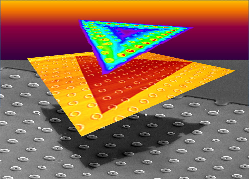
Researchers at Oak Ridge National Laboratory grew strain-tolerant, triangular, monolayer crystals of tungsten disulfide on silicon dioxide substrates patterned with donut-shaped pillars, as shown in scanning electron microscope (bottom) and atomic force microscope (middle) image elements. The curvature of the pillars induces strain in the overlying crystals that locally alters their optoelectronic properties, as shown in bright regions of photoluminescence (top). Illustration by Christopher Rouleau/Oak Ridge National Laboratory, U.S. Dept. of Energy
Strain also influenced phonons, the collective vibrational excitations in material that affect the conduction of heat, electricity and sound. Tensile strain softened phonon modes, while compressive strain stiffened them.
Surprisingly, the crystals grew faster in the flat plains between donuts. Oak Ridge models showed the strain prompted additional nucleation sites between the obstacles. And when the crystals were removed from the substrate, the strain disappeared and no trace of the trench or donut patterns remained.
Yu said the new work continues a collaboration that started with patterning 2D materials onto cones. “In that paper we mainly explored how topography like a cone can create grain boundaries, essentially breaking the material up into two pieces,” he said. “Here, we’re mostly focusing on how the strain changes the bandgap or the properties, and how to avoid breaking up.”
Ideally, Yakobson said the work will lead to computational models that allow researchers to predict the characteristics of any 2D material on any kind of supporting surface. “An even greater challenge is to solve the inverse problem — that is, to determine the topography of the substrate, which would yield the specific pattern of strain desired for electronic, optical or magnetic functionality of the deposited atomic film,” he said.
Co-authors of the paper are Alexander Puretzky, Bernadeta Srijanto, Xufan Li, Masoud Mahjouri-Samani, Christopher Rouleau, Akinola Oyedele, Mina Yoon, Xiang Gao and Gyula Eres of Oak Ridge; Zhili Hu of Nanjing University of Aeronautics and Astronautics, China; and Mengkun Tian of the University of Tennessee. Wang is a postdoctoral research associate, Xiao a staff scientist and Geohegan leader of the Functional Hybrid Nanomaterials Group at the Center for Nanophase Materials Sciences at Oak Ridge. Yakobson is the Karl F. Hasselmann Professor of Materials Science and NanoEngineering and a professor of chemistry at Rice.
The U.S. Department of Energy (DOE) Office of Science, Basic Energy Sciences, Materials Sciences and Engineering Division; DOE’s Center for Nanophase Materials Sciences; DOE’s National Energy Research Scientific Computing Center, and the Office of Naval Research supported the research.
-30-
Read the abstract at https://advances.sciencemag.org/content/5/5/eaav4028
Follow Rice News and Media Relations via Twitter @RiceUNews
Video:
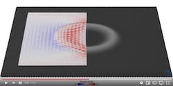
CAPTION: A model by Rice University shows how compressive strain (blue) and tensile strain (red) form as a growing two-dimensional crystal conforms to a micron-scale “donut” pattern on a substrate. The strain makes the hole a semiconductor and a possible source of single-photon emission. (Video by Nitant Gupta/Henry Yu/Yakobson Research Group)
Related materials:
2D crystals conforming to 3D curves create strain for engineering quantum devices: https://www.ornl.gov/news/2d-crystals-conforming-3d-curves-create-strain-engineering-quantum-devices
Imperfections make photons perfect for quantum computing: http://news.rice.edu/2018/12/17/imperfections-make-photons-perfect-for-quantum-computing-2/
Landscapes give latitude to 2D material designers: http://news.rice.edu/2017/08/09/landscapes-give-latitude-to-2-d-material-designers-2/
Yakobson Research Group: https://biygroup.blogs.rice.edu
Rice Department of Materials Science and Nanoengineering: https://msne.rice.edu
George R. Brown School of Engineering: https://engineering.rice.edu
Images for download:
https://news2.rice.edu/files/2019/05/0604_STRAIN-3-web.jpg
Rice University graduate students Nitant Gupta, left, and Henry Yu performed theoretical calculations that showed how the “donuts” on a growth substrate influence the electronic behavior of two-dimensional materials. The resulting localized strain could help researchers tune the properties of the material for applications like quantum information systems. (Credit: Jeff Fitlow/Rice University)
https://news2.rice.edu/files/2019/05/0604_STRAIN-1-WEB.jpg
Growing two-dimensional crystals over an array of micron-scale “donuts” may lead to tailored materials for quantum information processing and other novel electronics, according to scientists at Oak Ridge National Laboratory and Rice University. (Credit: Illustration by Henry Yu/Rice University)
https://news2.rice.edu/files/2019/05/0604_STRAIN-2-web.jpg
Researchers at Oak Ridge National Laboratory grew strain-tolerant, triangular, monolayer crystals of tungsten disulfide on silicon dioxide substrates patterned with donut-shaped pillars, as shown in scanning electron microscope (bottom) and atomic force microscope (middle) image elements. The curvature of the pillars induces strain in the overlying crystals that locally alters their optoelectronic properties, as shown in bright regions of photoluminescence (top). (Credit: Christopher Rouleau/Oak Ridge National Laboratory, U.S. Dept. of Energy)
Located on a 300-acre forested campus in Houston, Rice University is consistently ranked among the nation’s top 20 universities by U.S. News & World Report. Rice has highly respected schools of Architecture, Business, Continuing Studies, Engineering, Humanities, Music, Natural Sciences and Social Sciences and is home to the Baker Institute for Public Policy. With 3,962 undergraduates and 3,027 graduate students, Rice’s undergraduate student-to-faculty ratio is just under 6-to-1. Its residential college system builds close-knit communities and lifelong friendships, just one reason why Rice is ranked No. 1 for lots of race/class interaction and No. 2 for quality of life by the Princeton Review. Rice is also rated as a best value among private universities by Kiplinger’s Personal Finance.

