Editor’s note: Links to images for download appear at the end of this release.
David Ruth
713-348-6327
david@rice.edu
Mike Williams
713-348-6728
mikewilliams@rice.edu
‘Pixel’ engineered electronics have growth potential
Rice, Oak Ridge, Vanderbilt, Penn scientists lead creation of atom-scale semiconducting composites
HOUSTON – (Sept. 29, 2014) – A little change in temperature makes a big difference for growing a new generation of hybrid atomic-layer structures, according to scientists at Rice University, Oak Ridge National Laboratory, Vanderbilt University and Pennsylvania State University.
Rice scientists led the first single-step growth of self-assembled hybrid layers made of two elements that can either be side by side and one-atom thick or stacked atop each other. The structure’s final form can be tuned by changing the growth temperature.
The discovery reported online this week in Nature Materials could lead to what Rice materials scientist Pulickel Ajayan calls “pixel engineering”: atomically thin semiconductors with no limit to their potential for use in optoelectronic devices.
The researchers led by Ajayan and Wu Zhou, a materials scientist at Oak Ridge, discovered the interesting new composites when they combined the growth of two-dimensional molybdenum disulfide and tungsten disulfide through chemical vapor deposition. In this process, specific gases are heated in a furnace, where their atoms gather in an orderly fashion around a catalyst to form the crystalline material.
High-temperature growth – about 850 degrees Celsius (1,563 degrees Fahrenheit) – yielded vertically stacked bilayers, with tungsten on top. At lower temperatures, about 650 degrees C (1,202 degrees F), the crystal lattices preferred to grow side by side. The interfaces in either material are sharp and clean, as seen under a scanning electron microscope and in spectroscopic studies.
“With the advent of 2-D layered materials, people are trying to build artificial structures using graphene and now dichalcogenides as building blocks,” Ajayan said. Because graphene is atomically thin and flat and dichalcogenides like molybdenum disulfide are not quite that flat, there is some incompatibility when these are grown together — but two dichalcogenides with different compositions could be compatible. “We show that depending on the conditions, we can combine two dichalcogenides to grow either in-plane hybrid or in stacks.”
The monolayer composites have small but stable band gaps, while the stacked composite layers show modified electronic properties such as enhanced photoluminescence, which will be useful for electronics that rely on optical signals.
“What’s even more interesting is that the layered structure has a particular lock-in stacking order,” Zhou said. “When you stack 2-D materials by transferring layers, there’s no way to control their orientation to one another. That impacts their electronic properties. In this paper, we demonstrate that in a certain window, we can get a particular stacking order during growth, with a particular orientation.”
The new materials could be used for vertically stacked field-effect transistors as well as electronic devices only a few atoms thick, he said.
“We should be able to tweak certain regions to control certain functions, like light or terahertz emission,” said Robert Vajtai of Rice, a co-author of the study. “The whole idea, really, is to create domains with different electronic characters within a single layer.”
“Our goal is to build fully functional electronic devices on a single plane, or maybe a few layers,” added Mauricio Terrones, a co-author from Penn State. “What we’ve accomplished means that pretty much any architecture for devices is now possible on a single atomic layer. And that’s remarkable.”
Co-authors are graduate students Yongji Gong, Gang Shi, Sidong Lei and Gonglan Ye and postdoctoral researcher Xiaolong Zou; Jun Lou, an associate professor and associate department chair of materials science and nanoengineering; and Boris Yakobson, the Karl F. Hasselmann Professor of Materials Science and NanoEngineering and a professor of chemistry, all of Rice; Junhao Lin and Sokrates Pantelides of Oak Ridge and Vanderbilt University; Xingli Wang, Beng Kang Tay and Zheng Liu of Nanyang Technological University, Singapore; graduate student Zhong Lin of Pennsylvania State University; and Humberto Terrones, the Rayleigh Endowed Chair Professor of Physics at Rensselaer Polytechnic Institute.
Vajtai is a faculty fellow at Rice. Mauricio Terrones is a professor of physics, chemistry, materials science and engineering at Penn State. Ajayan is Rice’s Benjamin M. and Mary Greenwood Anderson Professor in Mechanical Engineering and Materials Science and of chemistry and chair of the Department of Materials Science and NanoEngineering.
The Army Research Office, the Department of Energy, the National Science Foundation, the Microelectronics Advanced Research Corp., the Defense Advanced Research Projects Agency, the U.S. Office of Naval Research and the Ministry of Education Academic Research Fund and Silicon Technologies Center of Excellence, Singapore, supported the research.
-30-
Read the abstract at http://dx.doi.org/10.1038/nmat4091
Follow Rice News and Media Relations via Twitter @RiceUNews
Related Materials:
Ajayan Group: http://ajayan.rice.edu
The STEM Group at Oak Ridge National Laboratory (Zhou): http://stem.ornl.gov/index.shtml
Mauricio Terrones: http://www.phys.psu.edu/people/mut11
Rice Department of Materials Science and NanoEngineering: http://msne.rice.edu
Images for download:

https://news2.rice.edu/files/2014/09/0929_STRUCTURES-1-web.jpg
Stacked (top) and in-plane nanomaterials self-assemble in two ways, depending on the temperature at which they’re grown, according to Rice University researchers who led the project. The semiconducting materials show promise for a new generation of “pixel” electronics. In the illustration, green spheres are tungsten, purple are molybdenum and yellow are sulfur. (Credit: Ajayan Group/Rice University)

https://news2.rice.edu/files/2014/09/0929_STRUCTURES-2-web.jpg
This image shows the interface between elements of the in-plane material created by scientists at Rice University and their colleagues. Tungsten disulfide (orange) and molybdenum disulfide (blue) molecules self assemble into either single- or multiple-layer materials, depending on growth temperature. (Credit: Yongji Gong and Junhao Lin)

https://news2.rice.edu/files/2014/09/0929_STRUCTURES-3-web.jpg
This atomic-resolution image shows the sharp line between tungsten disulfide (brighter) and molybdenum disulfide (darker) in a new material made in a collaboration led by Rice University. The two-dimensional material shows promise for nanoelectronic applications. (Credit: Oak Ridge National Laboratory)

https://news2.rice.edu/files/2014/09/0929_STRUCTURES-4-web.jpg
This atomic-resolution image shows the sharp line between tungsten disulfide (brighter) and molybdenum disulfide (darker) in a new material made in a collaboration led by Rice University. The two-dimensional material shows promise for nanoelectronic applications. (Credit: Oak Ridge National Laboratory)
https://news2.rice.edu/files/2014/09/0929_STRUCTURES-5-web.jpg
Stacked heterostructures of tungsten disulfide and molybdenum disulfide were grown in experiments at Rice University. The form of the structures depends on the growth temperature: Higher temperatures resulted in stacked structures, while lower temperatures produced in-plane structures. The material may be useful for nanoelectronic applications. (Credit: Ajayan Group/Rice University)

https://news2.rice.edu/files/2014/09/0929_STRUCTURES-6-web.jpg
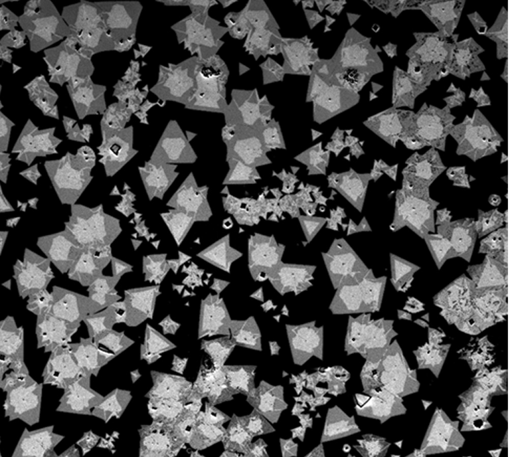
An image of a vertically stacked heterostructure of tungsten disulfide (bottom) and molybdenum disulfide, created in an experiment at Rice University. The structures self assemble in a furnace at 850 degrees Celsius. Lower temperatures formed single-layer heterostructures. The structure is about 20 microns across. (Credit: Ajayan Group/Rice University)

https://news2.rice.edu/files/2014/09/0929_STRUCTURES-7-web.jpg
An image of an in-plane heterostructure of tungsten disulfide and molybdenum disulfide, created in an experiment at Rice University. The structures self assemble in a furnace at 650 degrees Celsius. Higher temperatures formed stacked heterostructures. The structure is about 20 microns across. (Credit: Ajayan Group/Rice University)
Located on a 300-acre forested campus in Houston, Rice University is consistently ranked among the nation’s top 20 universities by U.S. News & World Report. Rice has highly respected schools of Architecture, Business, Continuing Studies, Engineering, Humanities, Music, Natural Sciences and Social Sciences and is home to the Baker Institute for Public Policy. With 3,920 undergraduates and 2,567 graduate students, Rice’s undergraduate student-to-faculty ratio is just over 6-to-1. Its residential college system builds close-knit communities and lifelong friendships, just one reason why Rice is highly ranked for best quality of life by the Princeton Review and for best value among private universities by Kiplinger’s Personal Finance. To read “What they’re saying about Rice,” go here.

